Description of work
Future wireless systems will have to achieve self-reconfigurable operations for real time efficient optimization of their performances. RF-MEMS switches will allow to face this challenge and open the route towards reconfigurability of high power systems, but their reliability is still nowadays an issue. The aim of NANOCOM project is to develop a new approach for future generation of smart systems by introducing nanostructured materials capacitive MEMS to improve the reliability by one order of magnitude. NANOCOM aims to address the dielectric charging effect which limits the lifetime and to enhance the thermal performances of the device, increasing the power handling capability.
The main objectives of NANOCOM are:
1) explore new nanostructured materials to be used as dielectrics in RF-MEMS devices to achieve higher reliable devices by minimizing charging effects and improving thermal dissipation under high power. High-k dielectrics such as PZT with a fine control of the nanostructure and composites, aligned Carbon Nanotubes in a Si3N4 matrix and doped poly crystalline diamond as well as diamond nanopillars.
2) develop the design methodologies and technological process to achieve the integration of these MEMS switches in phase shifters and SPDT devices.
3) develop gas and pressure sensors and actuators of unprecedented performance that can be integrated with RF components of the same type to perform complex functions such as sensing/actuating combined with wireless transmission of data.
Components of this type can improve the energy efficiency of systems by leading to efficient power supplies with intelligent energy control while allowing at the same time an increase of safety and functionality.
Demonstrators will be fabricated by implementing them in a reconfigurable T/R module, a tunable filter and a nitride-based sensor and actuator. The consortium possesses the experience to undertake this ambitious task. It is composed of 16 partners originating from 6 European countries half of them is industrial representation and half of them coming from research institute and university. It merges outstanding research groups with expertise in the fields of interest from the material to the system design and fabrication..
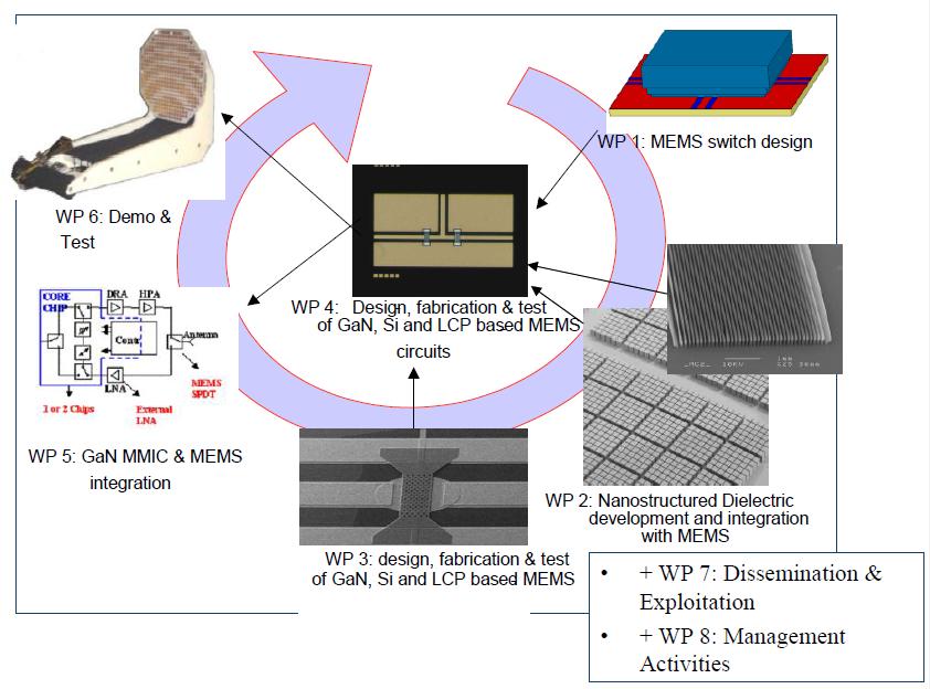
The organizational structure is shown in Figure below:
There are five discrete but interrelated work packages of development activities (WPs 1-5): RTD
activities are developed in WPs 1 to 5, while WP6 is devoted to demonstration activities:
Wp1 - MEMS and MiniMEMS switch design on GaN thin film, on LCP and on Si
Wp2 - Integration of new nanostructured materials (as new dielectrics) in the existing MEMS technology:
- PZT thin layers (by Pulsed Laser Deposition) with improved performances in term of the electrical conductivity
- Aligned carbon nanotubes within a Si3N4 dielectric matrix
- Nanocrystalline diamond
- TiO2
Wp3 - Design , Fabrication and test of GaN , Si and LTC based MEMS and MiniMEMS switched capacitors and phased shifters for active antenna
Wp4 - Design, fabrication and test of GaN, LTC and Si based RF-MEMS circuits and LCP boards
Wp5 - Integration of GaN/Si based MMIC with RF-MEMS technology
Wp6 - Fabrication of demonstrators: smart active antenna, miniaturized reconfigurable front-end and a miniaturized piezo sensor and actuator based on III-Nitride materials
Wp7 - Dissemination of the results achieved towards scientific community as well as industry in the field of nanosystems. Identifiable means: website, workshops, e-newsletter, promotion via refereed journals and international conferences.
Wp8 - Finally, management activities are grouped into work package 8

